
By Bill Taylor
Director of Semiconductor Operations, FuzeHub
At FuzeHub, we see a clear opportunity to strengthen New York State’s semiconductor ecosystem by connecting its diverse industry players and filling a critical gap—one that matters not just to the state, but to the nation. While New York is already recognized for its chip-making expertise, the next frontier is advanced packaging, and that is where NYS has the opportunity to lead.
Why Packaging Matters
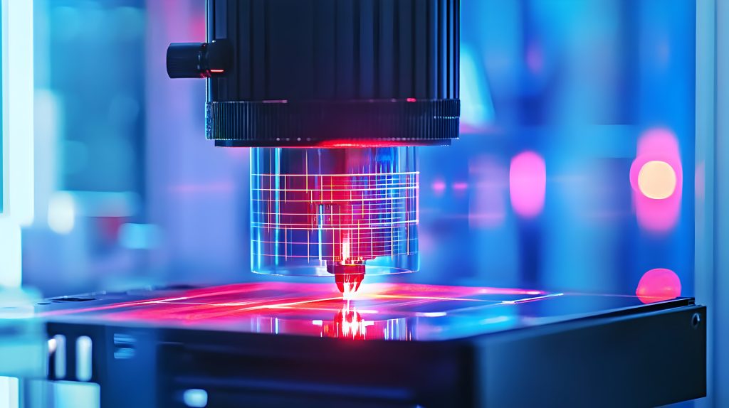
In microelectronics, manufacturing the chip itself is only part of the challenge. Virtually every electronic system—smartphones, networking equipment, vehicles, industrial controls, even everyday appliances—relies on multiple chips working together. These chips are assembled into what’s known as a package, which enables them to communicate efficiently. Packages are then mounted onto printed circuit boards (PCBs), forming the foundation of modern electronics.
For decades, the industry focused on making chips smaller, faster, and more powerful. Today, the same race is happening in packaging. Advanced packaging is no longer just about connectivity—it directly impacts signal timing, power efficiency, thermal performance, and ultimately system functionality.
The Next Leap: Structures and Materials
There are two primary levers for improving package performance: interconnect structures and materials.
Traditional approaches rely on either wire bonds or solder bumps to connect chips to substrates. While effective, these structures consume valuable space and face limitations as interconnect densities continue to rise. The industry’s long-term goal is a fully planar interface—where copper and insulating regions on a chip align precisely with matching patterns on the substrate, enabling ultra-dense, high-performance connections without bulky structures.
Materials are just as important. Most packages today use polymer substrates with copper wiring layers. These materials have remained largely unchanged for decades, but as data rates climb and chip-to-chip distances shrink, polymers are increasingly becoming a bottleneck.
Why Glass Is the Future
The industry is now transitioning toward glass substrates, and for good reason. Compared to polymers, glass:
-
Absorbs far less RF signal
-
Maintains exceptional flatness
After years of discussion, glass is finally moving from concept to reality—driven by major industry adoption and reinforced by significant federal investment through the CHIPS Act.
We see an even bigger opportunity: extending glass beyond the substrate into the redistribution layers (RDLs)—the wiring layers that connect chips within the package. Glass-on-glass packaging offers major advantages:
-
Up to 10× lower RF loss compared to polymer
-
Much finer feature sizes, enabling higher interconnect density
-
Well-established copper-to-glass bonding techniques
-
Compatibility with industry-standard semiconductor processes
-
Proven long-term reliability, critical for commercial and defense applications
By eliminating material mismatches between polymer and glass, many thermal and reliability challenges disappear.
Enabling the Future of Photonics and AI
Glass-based packaging also unlocks new possibilities in photonics, where data is transmitted using light instead of electrons. Photonics is a key enabler for next-generation AI systems, particularly through co-packaged optics, where photonic chips are integrated alongside advanced logic processors.
Because photonic devices are already built using glass-based waveguides, a glass-on-glass packaging platform dramatically simplifies integration, improves performance, and accelerates development timelines.
Building a National Resource in New York
FuzeHub’s vision is to establish a facility that enables small design houses, startups, and U.S. government programs to develop glass-based packaging using production-quality tools. This approach allows innovators to prototype, validate, and then seamlessly transfer their designs to high-volume manufacturing partners.
New York State has long been a leader in semiconductor manufacturing. By expanding into advanced, glass-based packaging, we can ensure that leadership continues—strengthening domestic supply chains and supporting the next generation of microelectronics innovation.
Join the Glass4Chips Initiative
This vision comes together through Glass4Chips, a growing initiative to unite manufacturers, researchers, startups, and public partners around advancing glass-based microelectronics and packaging in the United States. Glass4Chips is focused on building collaboration, shared infrastructure, and a clear pathway from innovation to production.
If you’re interested in shaping the future of advanced packaging, photonics, and semiconductor manufacturing, for glass-based microelectronics we invite you to join the effort and learn more at https://upstatemakes.org/